High Quality Metal Core Print Circuit Board Processing PCB Copper Base PCB Factory
Parameters: Layers: 1 Thicknes: 1.6±0.12mm Min. Hole Size: 0.5mm Surface Treatment: OSP Applications LED, LIGHT. Our mai
Description
Basic Info
| Model NO. | UC-3582 |
| Application | Consumer Electronics |
| Mechanical Rigid | Rigid |
| Material | Aluminum |
| Brand | Uc |
| Layers | 1/2 |
| Base | Aluminum |
| Material Finished Thickness | 1.6mm |
| Finished Copper Thickness | 1/2 Oz |
| Surface Treatment | Immersion Gold/HASL Lead Free/OPS/ Immersion Silve |
| Solder Mask Color | White |
| Screen Color | Black |
| PCB Testing | E-Testing; Flying Probe Testing |
| Lead Time | 5+ Working Days |
| Ipc Standards | Ipc Class II |
| Transport Package | Vacuum Package |
| Specification | UL(US&Canada). ISO. RoHs, TS, SGS |
| Trademark | UC |
| Origin | Shenzhen, China |
| HS Code | 8534009000 |
| Production Capacity | 20000 Sqm/Month |
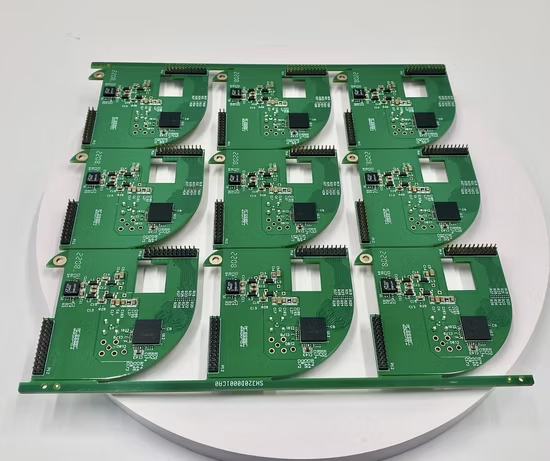
Product Description
Parameters:Layers: 1
Thicknes: 1.6±0.12mm
Min. Hole Size: 0.5mm
Surface Treatment: OSP
Applications
LED, LIGHT.
Our main products range from Multilayer PCB,High frequency PCB, Metal base PCB, Hi-Tg heavy copper foil PCB and Mixed Dielectric base PCB, HDI, rigid-flex PCB,and many other customized PCB with special performance which are widely used in Communication, power supply, computer, consumer electronics, industrial control, medical device, Aeronautics and Astronautics high technology field and spread over America, Europe and some Asia Districts, achieving their satisfication. Ucreate has been certificated with ISO9001, ISO14001, UL from US and Canada, all of our products are with ROHS certification.
Technical Capabilities:
| Items | Speci. | Remark | |
| Max panel size | 32" x 20.5"(800mm x 520mm) | ||
| Min trace width/ space (inner layer) | 4mil/4mil(0.1mm/0.1mm) | ||
| Min PAD (inner layer) | 5 mil(0.13mm) | hole ring width | |
| Min thickness(inner layer) | 4 mil(0.1mm) | without copper | |
| Inner copper thickness | 1~4 oz | ||
| Outer copper thickness | 0.5~6 oz | ||
| Finished board thickness | 0.4-3.2 mm | ||
Board thickness tolerance control | ±0.10 mm | ±0.10 mm | 1~4 L |
| ±10% | ±10% | 6~8 L | |
| ±10% | ±10% | ≥10 L | |
| Inner layer treatment | brown oxidation | ||
| Layer count Capability | 1-30 LAYER | ||
| alignment between ML | ±2mil | ||
| Min drilling | 0.15 mm | ||
| Min finished hole | 0.1 mm | ||
| Hole precision | ±2 mil(±50 um) | ||
| tolerance for Slot | ±3 mil(±75 um) | ||
| tolerance for PTH | ±3 mil(±75um) | ||
| tolerance for NPTH | ±2mil(±50um) | ||
| Max Aspect Ratio for PTH | 8:1 | ||
| Hole wall copper thickness | 15-50um | ||
| Alignment of outer layers | 4mil/4mil | ||
| Min trace width/space for outer layer | 4mil/4mil | ||
| Tolerance of Etching | +/-10% | ||
| Thickness of solder mask | on trace | 0.4-1.2mil(10-30um) | |
| at trace corner | ≥0.2mil(5um) | ||
| On base material | ≤+1.2mil Finished thickness | ||
| Hardness of solder mask | 6H | ||
| Alignment of solder mask film | ±2mil(+/-50um) | ||
| Min width of solder mask bridge | 4mil(100um) | ||
| Max hole with solder plug | 0.5mm | ||
| Surface finish | HAL (Lead or Lead free), immersion Gold, Immersion Nickel, Electric Gold finger, Electric Gold, OSP, Immersion Silver. | ||
| Max Nickel thickness for Gold finger | 280u"(7um) | ||
| Max gold thickness for Gold finger | 30u"(0.75um) | ||
| Nickel thickness in Immersion Gold | 120u"/240u"(3um/6um) | ||
| Gold thickness in Immersion Gold | 2u"/6u"(0.05um/0.15um) | ||
| Impedance control and its tolerance | 50±10%,75±10%,100±10% 110±10% | ||
| Trace Anti-stripped strength | ≥61B/in(≥107g/mm) | ||
| bow and twist | 0.75% | ||
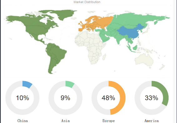
Market distributions:
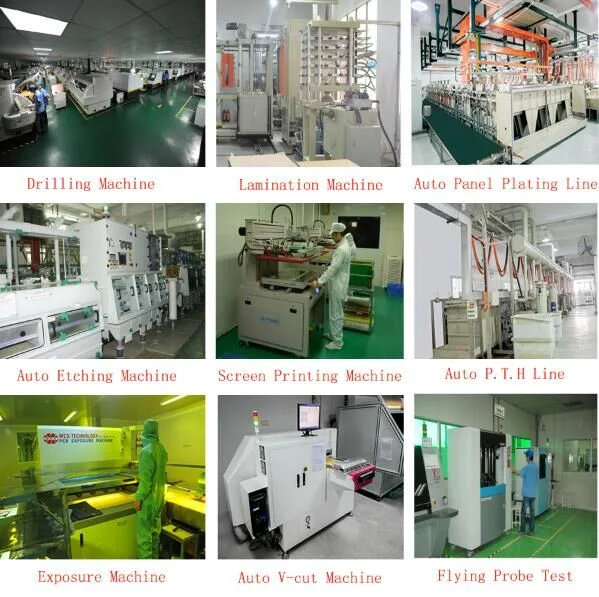
Product equipments:
Certificates:
Prev: Blind and Buried Holes Metal Core HDI High Tg/ Thick Copper Rigid-Flex Ceramic IC Test Flexible PCB
Next: PCBA Manufacturing Service Electronics Manufacturer Assembly SMT DIP PCB
Our Contact
Send now