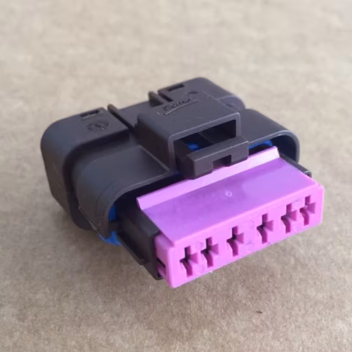
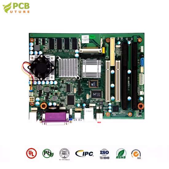
Shenzhen Manufacturer OEM Rigid Printed Circuit Board Metal Core Double-Sided PCB
Mitasemi is a manufacturer specializing in the production of high-quality PCB and PCBA, and is one of the earliest manuf
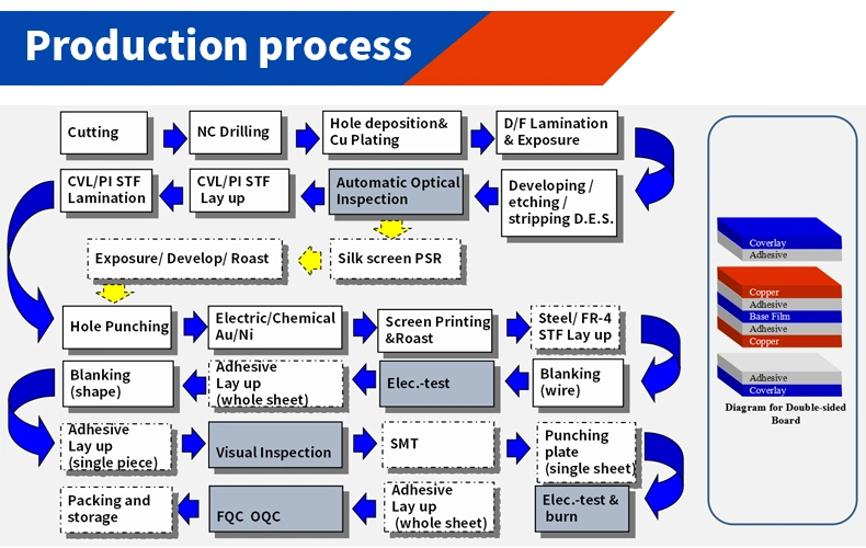
Description
Basic Info
| Model NO. | D02026A |
| Structure | Multilayer Rigid PCB |
| Dielectric | FR-4 |
| Material | Polyester Glass Fiber Mat Laminate |
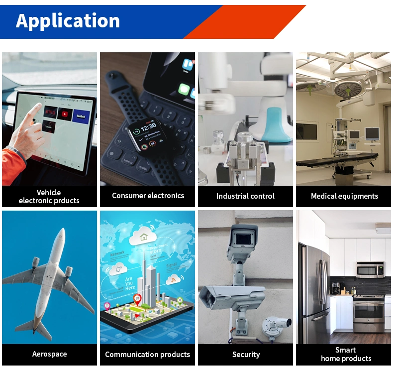
| Application | Medical Instruments |
| Flame Retardant Properties | V0 |
| Processing Technology | Electrolytic Foil |
| Production Process | Subtractive Process |
| Base Material | Copper |
| Insulation Materials | Organic Resin |
| Brand | Mitasemi |
| Line Width | Min 0.05mm |
| Copper Thickness | 1/3oz~6 Oz |
| Finished Board Thickness | FPC:1.0mm~1.6mm; PCB:0.1mm~3mm |
| MOQ | No |
| Service | OEM ODM |
| Transport Package | Vacuum Package |
| Specification | min 1*1mm |
| Trademark | Mitasemi |
| Origin | Guangdong China |
| Production Capacity | 20kk/Year |
Product Description
| ITEM | Classification | Specification | Remarks |
| Minimum linewidth / line spacing | Single/double-sided board | 0.035/0.035mm(1.4mil) | |
| Multilayer board | 0.06/0.06mm(2.4mil) | ||
| Minimum aperture | Drill hole | ø0.1mm(4mil) | |
| Punching | ø0.5mm | ||
| Dimensional tolerance | Linewidth | ±0.01mm(W≥0.05mm) | |
| Aperture | ±0.05mm(R≥0.6mm) | ||
| Interline accumulative spacing | ±0.05mm | ||
| Contour tolerance | ±0.05mm | ||
| Spacing between two holes | ±0.1mm | ||
| Fit tolerance of cover film | ±0.2mm | ||
| Slab/slab thickness | Single-sided slab | 0.08mm (1/2oz rubber calendaring) | |
| Double-sided slab | 0.1mm (1/3oz rubber-free electrolysis ) | ||
| Multilayer slab ability | 1-8 layers | ||
| Surface treatment | Electrolytic nickel/ gold | Ni (2-6µm) , Au (0.03-0.2µm) | |
| ENIG | Ni (2-6µm) , Au (0.03-0.15µm) | ||
| Palladium nickel gold | Ni (1-8µm) , pd (0.05-0.2µm) , Au (0.03-0.15µm) | ||
| Impedance | Differential impedance | 100±10%Ω | |
| Characteristic impedance | 50±10%Ω |
A:FPC: gerber files,quantities
PCB(printed circuit board): Quantity, Gerber file and Technic requirements(material,surface finish treatment, copper thickness,board thickness ,...)
PCBA(printed circuit board assembly): PCB information, BOM, (Testing documents...)
Q2:What is the lead time ?
A:(1)Sample
1-2 Layers: 5 to 7working days
4-8 Layers: 10 working days
(2)Mass production: 15~30days
Q3:What is your minimum order quantity(MOQ) ?
A: There is no MOQ in Mitasemi.We are able to handle Small as well as large volume production with flexibility.
Q4:Are my files safe?
A: Your files are held in complete safety and security.We protect the intellectual property for our customers in the whole process.. All documents from customers are never shared with any third parties.
Q5:Shipping cost?
A: The shipping cost is determined by the destination, weight, packing size of the goods. Please let us know if you need us to quote you the shipping cost.
Q6:Are you factory ?
A:Yes,we are a factory.
Our Contact
Send now